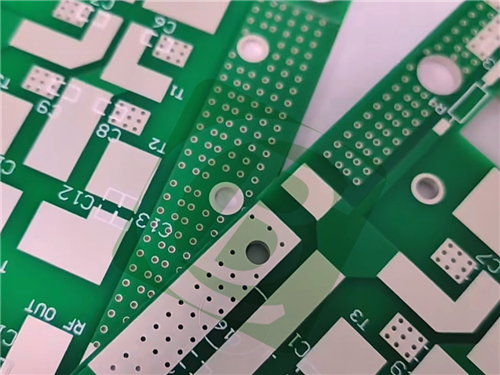
| MOQ: | 1 PCS |
| τιμή: | USD9.99-99.99 |
| Τυπική συσκευασία: | Τσάντες κενού+χαρτοκιβώτια |
| Περίοδος παράδοσης: | 8-9 εργάσιμες ημέρες |
| Μέθοδος πληρωμής: | T/t |
| Ικανότητα εφοδιασμού: | 5000pcs το μήνα |
This 2-layer high-performance PCB is engineered for RF (Radio Frequency) applications, utilizing the advanced properties of RF-10 copper clad laminates to achieve exceptional electrical, thermal, and mechanical performance.
1. PCB Specifications
| Parameter | Specification |
| Base Material | RF-10 copper clad laminate (ceramic-filled PTFE with woven fiberglass reinforcement) |
| Layer Count | 2 layers (top and bottom copper layers) |
| Board Dimensions | 130mm × 60mm per unit, tolerance ±0.15mm |
| Trace & Space Specifications | Minimum trace width 5 mils, minimum trace spacing 7 mils |
| Hole Requirements | Minimum hole size 0.3mm; no blind vias |
| Finished Board Thickness | 0.6mm |
| Copper Weight | 1oz (1.4 mils or 35μm) for top and bottom layers |
| Via Plating | 20μm thick plating on vias |
| Surface Finish | Immersion silver |
| Silkscreen & Solder Mask - Top Layer | White silkscreen + Green solder mask |
| Silkscreen & Solder Mask - Bottom Layer | No silkscreen or solder mask |
| Quality Assurance | 100% electrical testing prior to shipment |
2. PCB Stack-up
| Layer | Thickness | Function |
| Top Copper Layer (Copper_layer_1) | 35μm (1oz) | Primary layer for signal traces and component pads |
| RF-10 Core | 20 mils (0.508mm) | Dielectric substrate enabling RF capabilities |
| Bottom Copper Layer (Copper_layer_2) | 35μm (1oz) | Supports ground planes or additional signal paths |
3. Quality Standards
Artwork Format: Gerber RS-274-X, the industry-standard format for PCB manufacturing, ensuring compatibility with most design software and fabrication processes
Quality Certification: Complies with IPC-Class-2 standards, meeting rigorous requirements for performance, reliability, and consistency in commercial and industrial applications
Global Availability: Available for customers worldwide, regardless of country or region, ensuring seamless access to our products
![]()
4. RF-10 Material: Key Features & Advantages
The PCB’s performance is rooted in the superior properties of RF-10 copper clad laminates, a composite of ceramic-filled PTFE and woven fiberglass. Below is a detailed overview of its features and benefits:
4.1 Critical Material Features
RF-10 is optimized for RF applications, with specifications that ensure consistent performance at high frequencies:
-Dielectric Constant (DK): 10.2 ± 0.3 at 10GHz (tight tolerance for predictable signal behavior)
-Dissipation Factor: 0.0025 at 10GHz (ultra-low signal loss, critical for high-frequency RF systems)
-Thermal Conductivity: 0.85 W/mk (unclad) (efficient heat dissipation to prevent component overheating)
-Coefficient of Thermal Expansion (CTE): x = 16 ppm/°C, y = 20 ppm/°C, z = 25 ppm/°C (low expansion to maintain structural integrity under temperature fluctuations)
-Moisture Absorption: 0.08% (minimal water uptake, preventing performance degradation in humid environments)
-Flammability Rating: V-0 (self-extinguishing, meeting safety standards for electronics)
4.2 Core Benefits of RF-10
These features translate to tangible advantages for both design engineers and end-users:
-Size Reduction for RF Circuits: High DK (10.2) allows for smaller circuit footprints, ideal for compact devices like GPS antennas or satellite components
-Exceptional Dimensional Stability: Woven fiberglass reinforcement and low CTE prevent warping or shifting, ensuring alignment with other components
-Tight DK Tolerance: ±0.3 variation ensures consistent signal propagation across the PCB, reducing design iterations
-Enhanced Thermal Management: High thermal conductivity protects sensitive RF components from overheating, extending lifespan
-Strong Copper Adhesion: Bonds well to smooth low-profile copper, minimizing delamination risks and ensuring long-term reliability
-Low Multi-Axis Expansion: x, y, and z CTE values reduce stress on solder joints and components during temperature cycles
-Cost-Effective Performance: Balances high-end RF capabilities with industry-acceptable delivery times and pricing, offering an excellent price/performance ratio
5.Applications
- Microstrip Patch Antennas
- GPS Antennas
- Passive Components (filters, couplers, power dividers)
- Aircraft Collision Avoidance Systems
- Satellite components
In summary, the 2-layer RF-10 PCB combines precise manufacturing, high-quality materials, and industry-compliant design to deliver a reliable, high-performance solution for critical RF applications. Its balance of size, performance, and cost makes it a versatile choice for engineers seeking to optimize their RF systems.
![]()